Manufacture Electronic PCB Boards
A circuit board is a rigid platform that allows electrical signals to be transmitted to and from components on the board. These conductive pathways, known as traces, are typically made of copper and are etched onto the surface of the board. The underlying substrate material provides strength to the circuit board and acts as an insulator between the different layers of copper. The most common PCB materials are fiberglass and epoxy resin. Other popular materials include polyimide, ceramics, and metal-core substrates. The latter are usually used for high-frequency or high power applications due to their superior heat dissipation capabilities.
The most basic electronic pcb board have one layer of copper foil on top of the substrate, and the thickness of the copper is commonly specified in ounces per square foot. A bare copper layer is prone to oxidation, which reduces its conductivity over time. To avoid this, the traces are typically coated with a thin layer of solder or gold. The coating also protects the copper from damage during manufacturing and assembly.
To create a circuit board design, engineers first use a CAD program to create a schematic diagram. From this the physical specifications of the components and their connections are determined. This data is then captured on a clear mylar sheet and photolithographically reproduced to create a “photomask.” The photomask is then placed over the blank copper-clad laminate. The manufacturing process then adds vias, plated-through holes that connect the different layers.
What Materials Are Used to Manufacture Electronic PCB Boards?
The remaining layers of a printed circuit board are copper-clad laminates. The most common is FR-4, a woven fiberglass cloth impregnated with an epoxy resin. It is flame retardant and has good insulation properties. It is also very durable and has a low moisture absorption rate. Several grades of FR-4 with differing properties are available.
FR-4 is also relatively inexpensive. However, it has a higher loss tangent than more expensive materials, which can cause signal degradation. Designers are also concerned about the ability of the copper to carry current at a given frequency. To increase current carrying capacity, designers can increase trace width, or make the copper thicker.
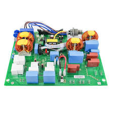
In addition to the standard traces, the surface of a circuit board may contain pads for connecting wires and component pins. These are identified with letters that indicate their function, such as PTH (plated through hole) or SMD (surface mount device). Some circuit boards have a solder paste stencil over the copper, which is used to line up and apply the solder paste during the assembly process.
Other features of a circuit board are buried traces, which are not exposed to the assembly process and are only used for power connections. Other hidden traces are used in communication between embedded processors. There are even specialty boards that allow for the interconnection of incompatible connectors, such as an SD card breakout board. A breakout board lets the user access an SD card’s data and power connectors without having to remove it from its enclosure.