Advantages of Using HDI CIRCUIT BOARDS
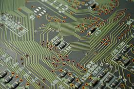
Printed circuit boards (PCBs) are the core of every electronic device. They have a variety of functions including data and power transmission, processing and control, and RF communication. HDI PCBs use high-density interconnect technology to incorporate smaller components in a smaller footprint, and are suited for many different applications. This technology also allows manufacturers to improve circuit board performance and reliability without sacrificing size.
hdi circuit boards have higher wiring density per circuit area, and can be manufactured with a much shorter production time than conventional PCBs. The increased performance that HDI circuit boards provide is especially useful in industries such as automotive, aerospace and military equipment, where space and weight are limited.
These types of PCBs are also often used in medical devices, such as pacemakers and miniaturized cameras. In these instances, it is important that the device is as small as possible while still allowing for functional operation. HDI circuit boards help in this endeavor by allowing for a reduction in size and weight, which can then reduce the cost of the final product.
What Are the Advantages of Using HDI CIRCUIT BOARDS?
The construction of an HDI PCB involves the etching of inner copper layers and then stacking them, separated by partially cured laminates with layers of prepreg on each side. This stack-up is then pressed and heated enough to liquify the prepreg, which then sticks the layers together. The number of sequential laminations required for an HDI PCB depends on the type of via structure and stackup height needed. The more layers that a PCB requires, the more expensive it will be to manufacture.
In addition to improved efficiency, HDI PCBs have better signal integrity than standard PCBs. This is because the conductive paths between components are shorter, which reduces signal reflections and cross-talk. Also, the use of blind and buried vias eliminates stubs that can cause interference, while filled and capped microvias placed directly in component solder lands minimize inductance in the distribution network.
Another reason why HDI PCBs are so popular is because they offer a more reliable platform than conventional circuit boards. The lower aspect ratios, microvias, and better electrical performance make them less susceptible to damage and stress from thermal expansion. This can lead to a longer lifespan for the finished product, and can reduce costs by reducing manufacturing and maintenance expenses.
The benefits of using HDI PCBs are clear, and the technology continues to grow in popularity as the demand for more efficient, smaller-sized electronics grows. This is particularly true in the automotive industry, where many new features — such as onboard WiFi and GPS, backup cameras, and advanced engine controls — are relying on HDI PCBs for their function. The technology is also being incorporated into military and aerospace equipment, as well as consumer electronic devices such as computers and phones. Regardless of the industry, the end result is a more compact and durable product that can achieve all the functionality that consumers are looking for.